Three researchers at Georgia Tech-CNRS IRL 2958, a joint international research laboratory based at Georgia Tech-Europe in Metz, France, were among a team that demonstrated cutting-edge 2D/single-crystalline 3D/2D (2D/C-3D/2D) Integration using a precise layer splitting technique to overcome drawbacks in ferroelectric materials use in electrostatic capacitors.
Metz, France
Three-dimensional (3D) hetero-integration technology is set to transform the field of electronics. Vertically stacking functional layers, creates novel 2D-3D circuit architectures with high integration density and unprecedented multifunctionality.
Three researchers at Georgia Tech-CNRS IRL 2958, a joint international research laboratory based at Georgia Tech-Europe in Metz, France, were among a team that demonstrated cutting-edge 2D/single-crystalline 3D/2D (2D/C-3D/2D) Integration using a precise layer splitting technique to overcome drawbacks in ferroelectric materials use in electrostatic capacitors.
Abdallah Ougazzaden, professor of Electrical and Computer Engineering at Georgia Tech, and president of Georgia Tech-Europe, Phuong Vuong, Georgia Tech-CNRS IRL 2958 researcher, and Suresh Sundaram, adjunct faculty in Georgia Tech’s School of Electrical and Computer Engineering, are co-authors on an April 19, 2024 research article in the journal, Science, entitled “High energy density in artificial heterostructures through relaxation time modulation.”
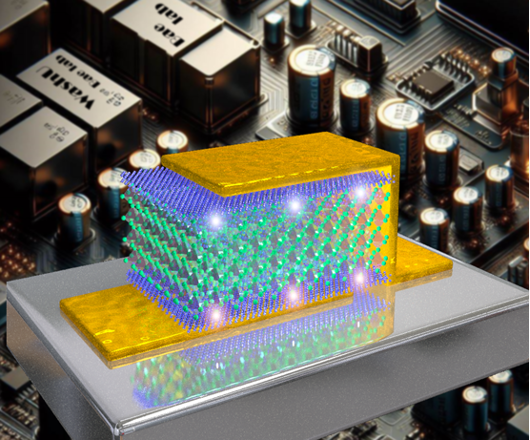
Ferroelectric materials used in electrostatic capacitors have unique advantages such as maximum polarization due to their higher electric susceptibilities related to dielectric constants, or permittivity, a measure of a material’s ability to store electrical energy. However, their high remnant polarization, the amount of polarization that remains in the material after the electric field is removed, limits how well they can store and release energy during the discharging process.
In the Science article, researchers demonstrated an innovative approach that sandwiches a single crystalline BTO (C-BTO) layer with 2D materials in the form of a freestanding membrane and effectively suppresses the remnant polarization of ferroelectric materials while maintaining the maximum polarization.
This ultra-thin vertical stacking technology was achieved using three different two-dimensional materials in combination with single crystalline BTO (C-BTO). Hexagonal boron nitride semiconductor was developed in the International Research Laboratory at GT-Europe, while graphene, and Molybdenum disulfide (MoS2) were developed at MIT.
These new 2D material technologies have a special type of bonding called van der Waals forces. On account of this, the layers can be easily separated to create components without needing any chemical etching or cutting processes.
“The 2D hexagonal boron nitride (h-BN) material that we are developing at Georgia Tech-CNRS IRL 2958 on large surfaces using the MOCVD epitaxial growth technique has demonstrated its significant potential in emerging technologies across various domains such as future quantum computers, biotechnology, flexible electronics, sensors, energy, and optogenetics.” said Ougazzaden, head of the h-BN project at Georgia Tech-CNRS IRL 2958,” adding, “We are currently working on some of these applications, and we hope to produce even more results and demonstrate new achievements."
Electrostatic capacitors, with their ability to store and release electrical energy quickly, find a wide range of applications across various fields of electronics and electrical engineering for energy storage, power conditioning etc.
In a similar collaboration, the same research team from Georgia Tech-CNRS IRL 2958 published a paper in December 2023, showing the first demonstration of the monolithic 3D integration of an artificial intelligence (AI) processor using two-dimensional (2D) materials.
This innovative integration approach combined six layers of transistor and memristor networks into a 3D nano-system. By stacking nanoscale materials made from 2D materials using bottom-up technology, the team created a fully integrated AI system.
The monolithic 3D method significantly improved processing efficiency by reducing time, voltage drops, latency, and footprint. In addition to offering a solution for electronic hetero-integration with 2D materials, broke new ground for advanced multifunctional processors and systems for AI applications and complex computing.
The team’s results on vertical hetero-integration were published in the scientific journal, Nature Materials, entitled, "Monolithic 3D Integration of 2D Materials-Based Electronics towards Ultimate Edge Computing Solutions.”
The researchers who contributed to the Science article discovered that when ferroelectric materials are combined in special structures (like 2D/C-3D/2D layers), it affects how much leftover charge a capacitor has and how well it can store energy. These insights will advance designs of high-energy capacitors using these materials. In the future, this could lead to more efficient and powerful energy storage systems.